Pad2Pad is a free PCB Design Software using which you can design a PCB circuit board. With Pad2Pad you can design PCB (Printed Circuit Board) for any circuit for 2/4 layers using a good predefined library of components and tools.
Pad2Pad offers custom size selection and the option to enable or disable Solder Mask and edit Silk Screen for PCB board. Also, Pad2Pad’s component library offers you lots of predefined components such as Capacitors, connectors, IC (Integrated Circuits) for different pins, Resistors, Transistor, and many more. The components are further divided for different ratings, which is great. Along, with this you can see the preview of the component symbol before placing them on board.
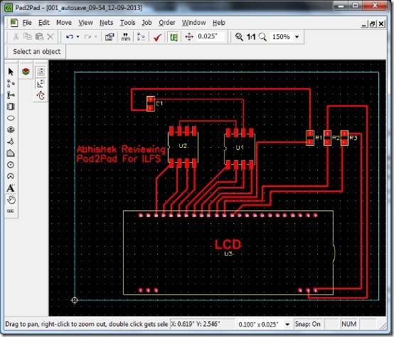
What I really like in Pad2Pad is that, it is really simple to use and you can get started with making your own PCB instantly, using this PCB design software. I have tested Pad2Pad by designing a random circuit using LCD, Resistors, and Capacitors and connected them using the trace. I have posted a screenshot below in which I have shown the PCB circuit design for the same.
Working with Pad2Pad PCB Design Software:
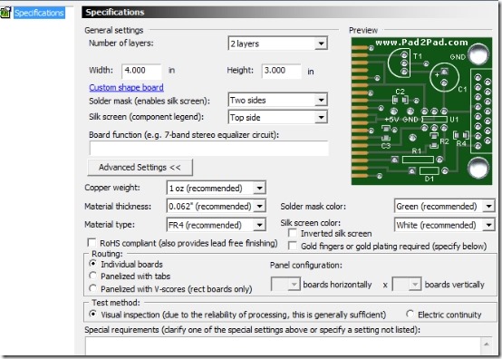
Pad2Pad is really simple to use and the user interface is simple to understand. When you first launch Pad2Pad you will be prompted to select the type of board on which you want to work. Pad2Pad offers you the option to select 2 and 4 layer boards, dimensions, and type of itching (Solder Mask). Furthermore, you can access advanced settings to access more options for the board.
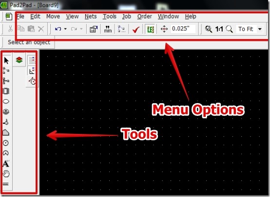
After you select the board you will have the user interface.
On the user interface you have toolbars from where you can select the components, traces, and other file options to work on the board.
After the PCB designing is complete you can print your work or save it as .pcb file.
Features of Pad2Pad:
- Option to select different layers for board.
- Logical Trace: It is a really interesting feature of Pad2Pad software. Using this option you can connect the terminals of a component without actually drawing the trace. And later you can just select Route Tool and you will have the terminals connected automatically. It’s a great feature as sometimes editing connections for traces can be tedious.
- Option to view Specific Layers: It’s another really helpful feature as in this option you can view the different layers of the PCB design. You can either view single or multiple layers for the PCB design.
- Option to create BOM (Parts list): After designing the circuit you can easily view all the components that you have used in designing the circuit.
- Option to import Netlist.
- Simplify traces with just one click.
- Zoom Option.
- Tools to draw the PCB design such as:
- Pad Tool.
- Multilayer Pad Tool.
- Tool to create polygon, circle, and arc.
- Text Tool to write text on the PCB design.
- Distance Tool to calculate distance in inches.
- Option to toggle inch/metric mode.
- Ruler for accurately placing the components.
You can also try another similar software for designing the circuit DIYLC.
Conclusion:
Pad2Pad is really simple to use and I was able to create some good designs using it. Pad2Pad has real interface and it worked flawlessly for me in Windows 7 . It’s a great tool for anyone who wants to design PCB circuit with good tools and components. Go ahead and try out Pad2Pad.


